


Idiomas
Páginas
Jurídico

MOTORES PASO A PASO
Los motores paso a paso son ideales para la construcción de mecanismos en donde se requieren movimientos muy precisos.
La característica principal de estos motores es el hecho de poder moverlos un paso a la vez por cada pulso que se le aplique. Este paso puede variar desde 90° hasta pequeños movimientos de tan solo 1.8°, es decir, que se necesitarán 4 pasos en el primer caso (90°) y 200 para el segundo caso (1.8°), para completar un giro completo de 360°.
Principio de funcionamiento
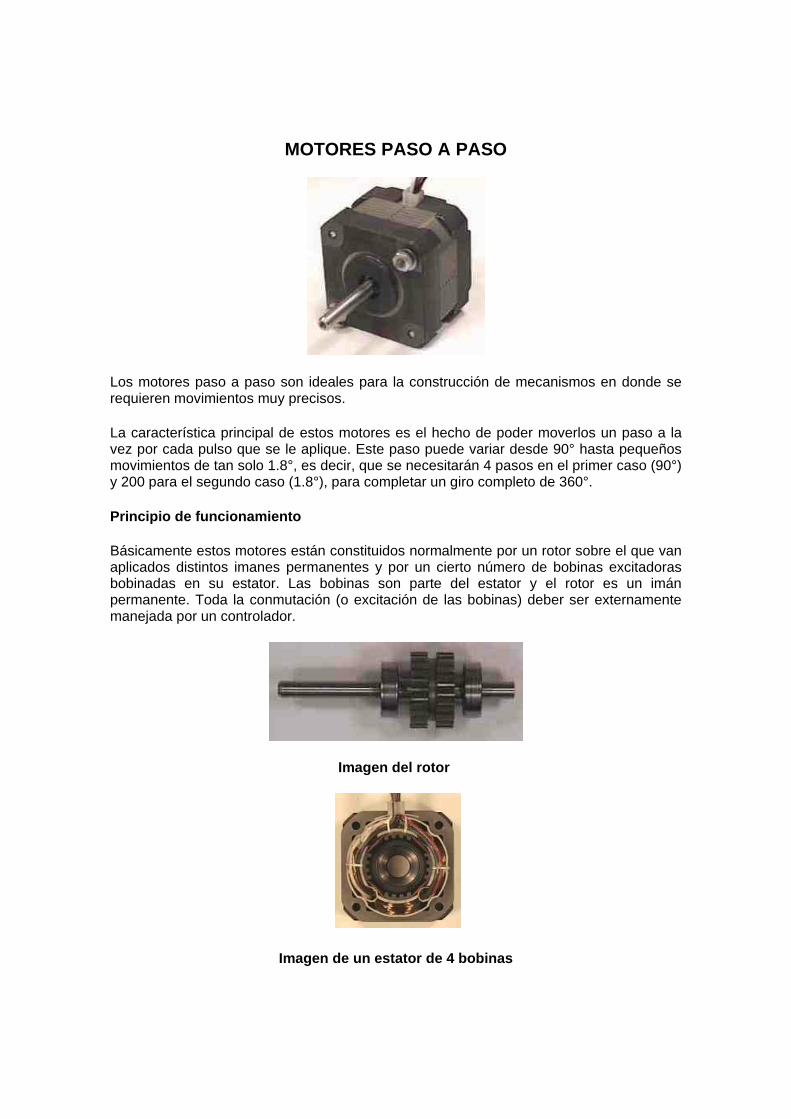
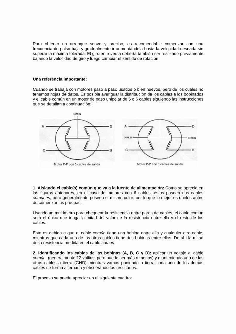
Básicamente estos motores están constituidos normalmente por un rotor sobre el que van aplicados distintos imanes permanentes y por un cierto número de bobinas excitadoras bobinadas en su estator. Las bobinas son parte del estator y el rotor es un imán permanente. Toda la conmutación (o excitación de las bobinas) deber ser externamente manejada por un controlador.
Imagen del rotor
Imagen de un estator de 4 bobinas

Existen dos tipos de motores paso a paso de imán permanente:
• Bipolar: Estos tiene generalmente cuatro cables de salida (ver figura 1). Necesitan ciertos trucos para ser controlados, debido a que requieren del cambio de dirección del flujo de corriente a través de las bobinas en la secuencia apropiada para realizar un movimiento. En la figura 3 podemos apreciar un ejemplo de control de estos motores mediante el uso de un puente en H (H-Bridge). Como se aprecia, será necesario un H-Bridge por cada bobina del motor, es decir que para controlar un motor Paso a Paso de 4 cables (dos bobinas), necesitaremos usar dos H-Bridges iguales al de la figura 3. El circuito de la figura 3 es a modo ilustrativo y no corresponde con exactitud a un H-Bridge. En general es recomendable el uso de H-Bridge integrados como son los casos del L293B (ver figura 3bis).

• Unipolar: Estos motores suelen tener 6 o 5 cables de salida, dependiendo de su conexión interna (ver figura 2). Este tipo se caracteriza por ser más simple de controlar. En la figura 4 podemos apreciar un ejemplo de conexionado para controlar un motor paso a paso unipolar mediante el uso de un ULN2803, el cual es una arreglo de 8 transistores tipo Darlington capaces de manejar cargas de hasta 500mA. Las entradas de activación (Activa A, B, C y D) pueden ser directamente activadas por un microcontrolador.
Secuencias para manejar motores paso a paso Bipolares
Como se dijo anteriormente, estos motores necesitan la inversión de la corriente que circula en sus bobinas en una secuencia determinada. Cada inversión de la polaridad provoca el movimiento del eje en un paso, cuyo sentido de giro está determinado por la secuencia seguida.
A continuación se puede ver la tabla con la secuencia necesaria para controlar motores paso a paso del tipo Bipolares:
PASO TERMINALES A B C D 1 +V -V +V -V 2 +V -V -V +V 3 -V +V -V +V 4 -V +V +V -V
Secuencias para manejar motores paso a paso Unipolares
Existen tres secuencias posibles para este tipo de motores, las cuales se detallan a continuación. Todas las secuencias comienzan nuevamente por el paso 1 una vez alcanzado el paso final (4 u 8). Para revertir el sentido de giro, simplemente se deben ejecutar las secuencias en modo inverso.

Secuencia Normal: Esta es la secuencia más usada y la que generalmente recomienda el fabricante. Con esta secuencia el motor avanza un paso por vez y debido a que siempre hay al menos dos bobinas activadas, se obtiene un alto torque de paso y de retención.
PASO Bobina A Bobina B Bobina C Bobina D
1 ON ON OFF OFF
2 OFF ON ON OFF
3 OFF OFF ON ON
4 ON OFF OFF ON
Secuencia del tipo wave drive: En esta secuencia se activa solo una bobina a la vez. En algunos motores esto brinda un funcionamiento más suave. Pero al estar solo una bobina activada, el torque de paso y retención es menor.
PASO Bobina A Bobina B Bobina C Bobina D
1 ON OFF OFF OFF

2 OFF ON OFF OFF
3 OFF OFF ON OFF
4 OFF OFF OFF ON
Secuencia del tipo medio paso: En esta secuencia se activan las bobinas de tal forma de brindar un movimiento igual a la mitad del paso real. Para ello se activan primero 2 bobinas y luego solo 1 y así sucesivamente. Como vemos en la tabla la secuencia completa consta de 8 movimientos en lugar de 4.
PASO Bobina A
Bobina B
Bobina C
Bobina D
1 ON OFF OFF OFF
2 ON ON OFF OFF

3 OFF ON OFF OFF
4 OFF ON ON OFF
5 OFF OFF ON OFF
6 OFF OFF ON ON
7 OFF OFF OFF ON
8 ON OFF OFF ON
Como comentario final, cabe destacar que debido a que los motores paso a paso son dispositivos mecánicos y como tal deben vencer ciertas inercias, el tiempo de duración y la frecuencia de los pulsos aplicados es un punto muy importante a tener en cuenta. En tal sentido el motor debe alcanzar el paso antes que la próxima secuencia de pulsos comience. Si la frecuencia de pulsos es muy elevada, el motor puede reaccionar en alguna de las siguientes formas:
• Puede que no realice ningún movimiento en absoluto. • Puede comenzar a vibrar pero sin llegar a girar. • Puede girar erráticamente. • O puede llegar a girar en sentido opuesto.
Para obtener un arranque suave y preciso, es recomendable comenzar con una frecuencia de pulso baja y gradualmente ir aumentándola hasta la velocidad deseada sin superar la máxima tolerada. El giro en reversa debería también ser realizado previamente bajando la velocidad de giro y luego cambiar el sentido de rotación.
Una referencia importante:
Cuando se trabaja con motores paso a paso usados o bien nuevos, pero de los cuales no tenemos hojas de datos. Es posible averiguar la distribución de los cables a los bobinados y el cable común en un motor de paso unipolar de 5 o 6 cables siguiendo las instrucciones que se detallan a continuación:
1. Aislando el cable(s) común que va a la fuente de alimentación: Como se aprecia en las figuras anteriores, en el caso de motores con 6 cables, estos poseen dos cables comunes, pero generalmente poseen el mismo color, por lo que lo mejor es unirlos antes de comenzar las pruebas.
Usando un multímetro para chequear la resistencia entre pares de cables, el cable común será el único que tenga la mitad del valor de la resistencia entre ella y el resto de los cables.
Esto es debido a que el cable común tiene una bobina entre ella y cualquier otro cable, mientras que cada uno de los otros cables tiene dos bobinas entre ellos. De ahí la mitad de la resistencia medida en el cable común.
2. Identificando los cables de las bobinas (A, B, C y D): aplicar un voltaje al cable común (generalmente 12 voltios, pero puede ser más o menos) y manteniendo uno de los otros cables a tierra (GND) mientras vamos poniendo a tierra cada uno de los demás cables de forma alternada y observando los resultados.
El proceso se puede apreciar en el siguiente cuadro:
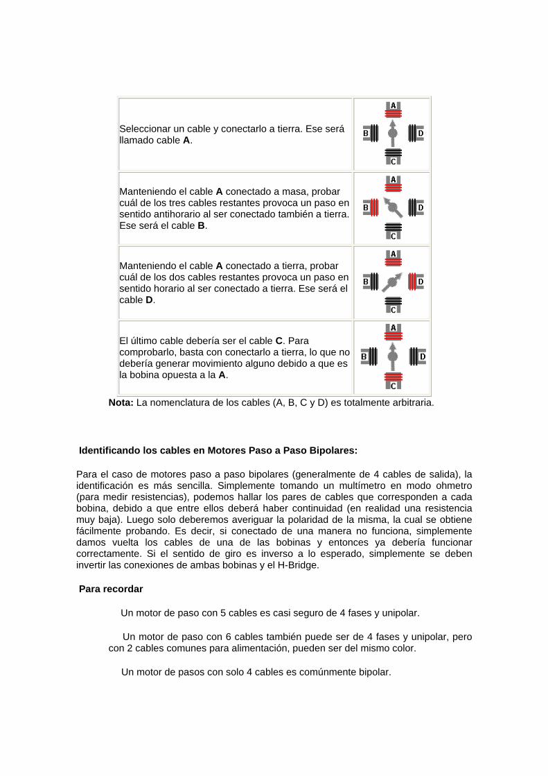
Seleccionar un cable y conectarlo a tierra. Ese será llamado cable A.
Manteniendo el cable A conectado a masa, probar cuál de los tres cables restantes provoca un paso en sentido antihorario al ser conectado también a tierra. Ese será el cable B.
Manteniendo el cable A conectado a tierra, probar cuál de los dos cables restantes provoca un paso en sentido horario al ser conectado a tierra. Ese será el cable D.
El último cable debería ser el cable C. Para comprobarlo, basta con conectarlo a tierra, lo que no debería generar movimiento alguno debido a que es la bobina opuesta a la A.
Nota: La nomenclatura de los cables (A, B, C y D) es totalmente arbitraria.
Identificando los cables en Motores Paso a Paso Bipolares:
Para el caso de motores paso a paso bipolares (generalmente de 4 cables de salida), la identificación es más sencilla. Simplemente tomando un multímetro en modo ohmetro (para medir resistencias), podemos hallar los pares de cables que corresponden a cada bobina, debido a que entre ellos deberá haber continuidad (en realidad una resistencia muy baja). Luego solo deberemos averiguar la polaridad de la misma, la cual se obtiene fácilmente probando. Es decir, si conectado de una manera no funciona, simplemente damos vuelta los cables de una de las bobinas y entonces ya debería funcionar correctamente. Si el sentido de giro es inverso a lo esperado, simplemente se deben invertir las conexiones de ambas bobinas y el H-Bridge.
Para recordar
Un motor de paso con 5 cables es casi seguro de 4 fases y unipolar.
Un motor de paso con 6 cables también puede ser de 4 fases y unipolar, pero con 2 cables comunes para alimentación, pueden ser del mismo color.
Un motor de pasos con solo 4 cables es comúnmente bipolar.

Referencias Utilizadas: [1] http://www.todorobot.com.ar/informacion/tutorial%20stepper/stepper-tutorial.htm [2] http://perso.wanadoo.es/luis_ju/ebasica2/mpp_01.html [3] http://www.cs.uiowa.edu/~jones/step/index.html

1/12
L293BL293E
July 2003
OUTPUT CURRENT 1A PER CHANNEL PEAK OUTPUT CURRENT 2A PER CHANNEL
(non repetitive) INHIBIT FACILITY HIGH NOISE IMMUNITY SEPARATE LOGIC SUPPLY OVERTEMPERATURE PROTECTION
DESCRIPTION
The L293B and L293E are quad push-pull driverscapable of delivering output currents to 1A perchannel. Each channel is controlled by a TTL-compatible logic input and each pair of drivers (afull bridge) is equipped with an inhibit input whichturns off all four transistors. A separate supply in-put is provided for the logic so that it may be runoff a lower voltage to reduce dissipation.
Additionally, the L293E has external connection of
sensing resistors, for switchmode control.
The L293B and L293E are package in 16 and 20-pin plastic DIPs respectively ; both use the fourcenter pins to conduct heat to the printed circuitboard.
DIP16 POWERDIP(16+2+2)
ORDERING NUMBERS:
L293B L293E
PUSH-PULL FOUR CHANNEL DRIVERS
PIN CONNECTION (Top view)
DIP16 - L293B
POWERDIP (16+2+2) - L293E

L293E L293B
2/12
BLOCK DIAGRAMS
DIP16 - L293B
POWERDIP (16+2+2) - L293E

3/12
L293E L293B
SCHEMATIC DIAGRAM
(*) In the L293 these points are not externally available. They are internally connected to the ground (substrate). O Pins of L293 () Pins of L293E.
ABSOLUTE MAXIMUM RATINGS
Symbol Parameter Value UnitVs Supply Voltage 36 VVss Logic Supply Voltage 36 V
Vi Input Voltage 7 VVinh Inhibit Voltage 7 V
Iout Peak Output Current (non repetitive t = 5ms) 2 APtot Total Power Dissipation at Tground-pins = 80°C 5 W
Tstg, Tj Storage and Junction Temperature –40 to +150 oC

L293E L293B
4/12
THERMAL DATA
ELECTRICAL CHARACTERISTCS
* See figure 1** Referred to L293E
TRUTH TABLE
(*) High output impedance(**) Relative to the considerate channel
Symbol Parameter Value Unit
Rth j-case Thermal Resistance Junction-case Max. 14 oC/W
Rth j-amb Thermal Resistance Junction-ambient Max. 80 oC/W
Symbol Parameter Test Condition Min. Typ. Max. Unit
Vs Supply Voltage Vss 36 V
Vss Logic Supply Voltage 4.5 36 V
Is Total Quiescent Supply Current Vi = L; Io = 0; Vinh = H 2 6 mA
Vi = h; Io = 0; Vinh = H 16 24 mA
Vinh = L 4 mA
Iss Total Quiescent Logic Supply Current
Vi = L; Io = 0; Vinh = H 44 60 mA
Vi = h; Io = 0; Vinh = H 16 22 mA
Vinh = L 16 24 mA
ViL Input Low Voltage -0.3 1.5 V
ViH Input High Voltage VSS ≤ 7V 2.3 Vss V
VSS > 7V 2.3 7 V
IiL Low Voltage Input Current Vil = 1.5V -10 µA
IiH High Voltage Input Current 2.3V ≤ VIH ≤ VSS - 0.6V 30 100 µA
VinhL Inhibit Low Voltage -0.3 1.5 V
VinhH Inhibit High Voltage VSS ≤7V 2.3 Vss V
VSS > 7V 2.3 7 V
IinhL Low Voltage Inhibit Current VinhL = 1.5V -30 -100 µA
IinhH High Voltage Inhibit Current 2.3V ≤VinhH≤ Vss- 0.6V ±10 µA
VCEsatH Source Output Saturation Voltage Io = -1A 1.4 1.8 V
VCEsatL Sink Output Saturation Voltage Io = 1A 1.2 1.8 V
VSENS Sensing Voltage (pins 4, 7, 14, 17) (**) 2 V
tr Rise Time 0.1 to 0.9 Vo (*) 250 ns
tf Fall Time 0.9 to 0.1 Vo (*) 250 ns
ton Turn-on Delay 0.5 Vi to 0.5 Vo (*) 750 ns
toff Turn-off Delay 0.5 Vi to 0.5 Vo (*) 200 ns
Vi (each channel) V o Vinh (**)
H H H
L L H
H X (*) L
L X (*) L

5/12
L293E L293B
Figure 1. Switching Timers
Figure 2. Saturation voltage versus Output Current
Figure 3. Source Saturation Voltage versus Ambient Temperature
Figure 4. Sink Saturation Voltage versus Ambient Temperature
Figure 5. Quiescent Logic Supply Current versus Logic Supply Voltage
L293E L293B
6/12
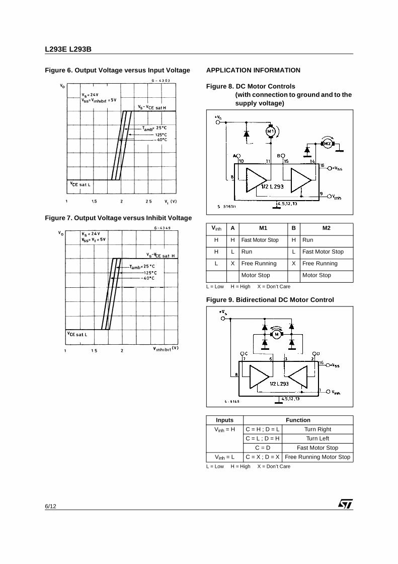
Figure 6. Output Voltage versus Input Voltage
Figure 7. Output Voltage versus Inhibit Voltage
APPLICATION INFORMATION
Figure 8. DC Motor Controls(with connection to ground and to the supply voltage)
L = Low H = High X = Don’t Care
Figure 9. Bidirectional DC Motor Control
L = Low H = High X = Don’t Care
Vinh A M1 B M2
H H Fast Motor Stop H Run
H L Run L Fast Motor Stop
L X Free Running X Free Running
Motor Stop Motor Stop
Inputs Function
Vinh = H C = H ; D = L Turn Right
C = L ; D = H Turn Left
C = D Fast Motor Stop
Vinh = L C = X ; D = X Free Running Motor Stop
7/12
L293E L293B
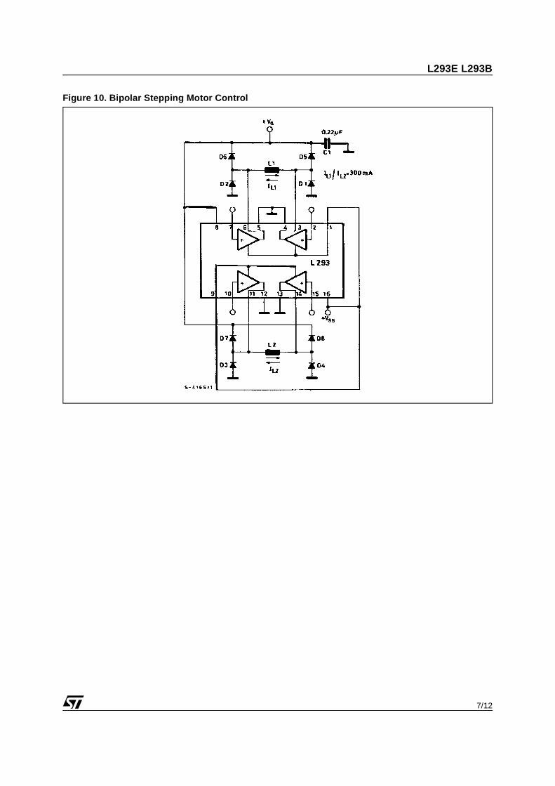
Figure 10. Bipolar Stepping Motor Control
L293E L293B
8/12
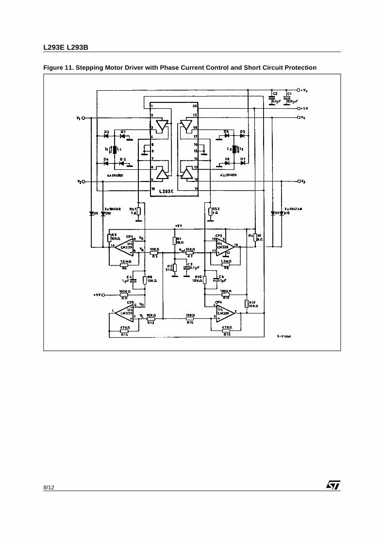
Figure 11. Stepping Motor Driver with Phase Current Control and Short Circuit Protection

9/12
L293E L293B
MOUNTING INSTRUCTIONS
The Rth j-amb of the L293B and the L293E can be reduced by soldering the GND pins to a suitable copperarea of the printed circuit board as shown in figure 12 or to an external heatsink (figure 13).
During soldering the pins temperature must not exceed 260°C and the soldering time must not be longerthan 12 seconds.
The external heatsink or printed circuit copper area must be connected to electrical ground.
Figure 12. Example of P.C. Board Copper Area which is Used as Heatsink
Figure 13. External Heatsink Mounting Example (R th = 30°C/W)
L293E L293B
10/12
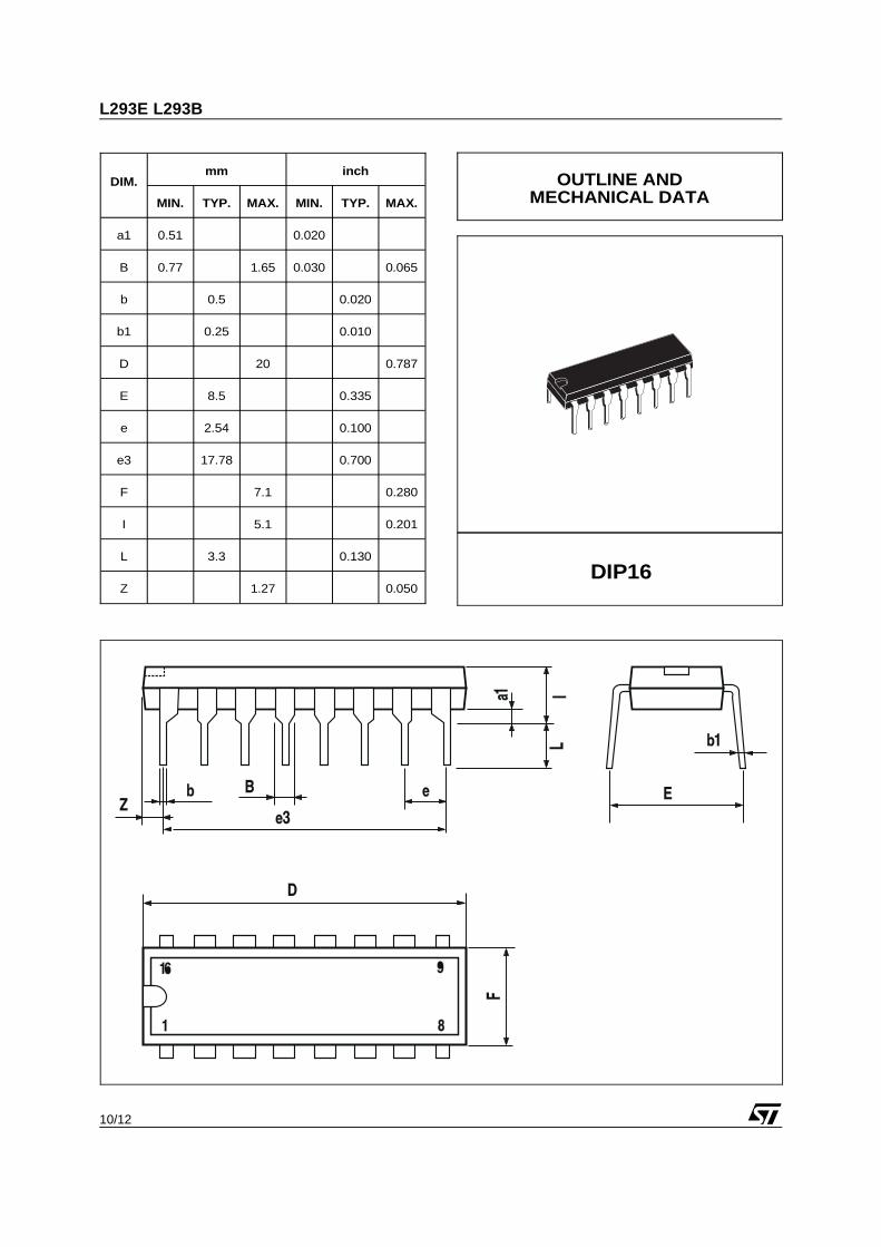
DIP16
DIM.mm inch
MIN. TYP. MAX. MIN. TYP. MAX.
a1 0.51 0.020
B 0.77 1.65 0.030 0.065
b 0.5 0.020
b1 0.25 0.010
D 20 0.787
E 8.5 0.335
e 2.54 0.100
e3 17.78 0.700
F 7.1 0.280
I 5.1 0.201
L 3.3 0.130
Z 1.27 0.050
OUTLINE ANDMECHANICAL DATA

11/12
L293E L293B
DIM.mm inch
MIN. TYP. MAX. MIN. TYP. MAX.
a1 0.51 0.020
B 0.85 1.40 0.033 0.055
b 0.50 0.020
b1 0.38 0.50 0.015 0.020
D 24.80 0.976
E 8.80 0.346
e 2.54 0.100
e3 22.86 0.900
F 7.10 0.280
I 5.10 0.201
L 3.30 0.130
Z 1.27 0.050Powerdip 20
OUTLINE ANDMECHANICAL DATA

Information furnished is believed to be accurate and reliable. However, STMicroelectronics assumes no responsibility for the consequencesof use of such information nor for any infringement of patents or other rights of third parties which may result from its use. No license is grantedby implication or otherwise under any patent or patent rights of STMicroelectronics. Specifications mentioned in this publication are subjectto change without notice. This publication supersedes and replaces all information previously supplied. STMicroelectronics products are notauthorized for use as critical components in life support devices or systems without express written approval of STMicroelectronics.
STMicroelectronics acknowledges the trademarks of all companies referred to in this document.
The ST logo is a registered trademark of STMicroelectronics© 2003 STMicroelectronics - All Rights Reserved
STMicroelectronics GROUP OF COMPANIESAustralia - Brazil - Canada - China - Finland - France - Germany - Hong Kong - India - Israel - Italy - Japan -Malaysia - Malta - Morocco -
Singapore - Spain - Sweden - Switzerland - United Kingdom - United States.http://www.st.com
12/12
L293E L293B
HIGH-VOLTAGE, HIGH-CURRENTDARLINGTON ARRAYS
FEATURES
TTL, DTL, PMOS, or CMOS Compatible Inputs Output Current to 500 mA Output Voltage to 95 V Transient-Protected Outputs Dual In-Line Package or Wide-Body Small-Outline Package
Data S
heet29304.3E
*
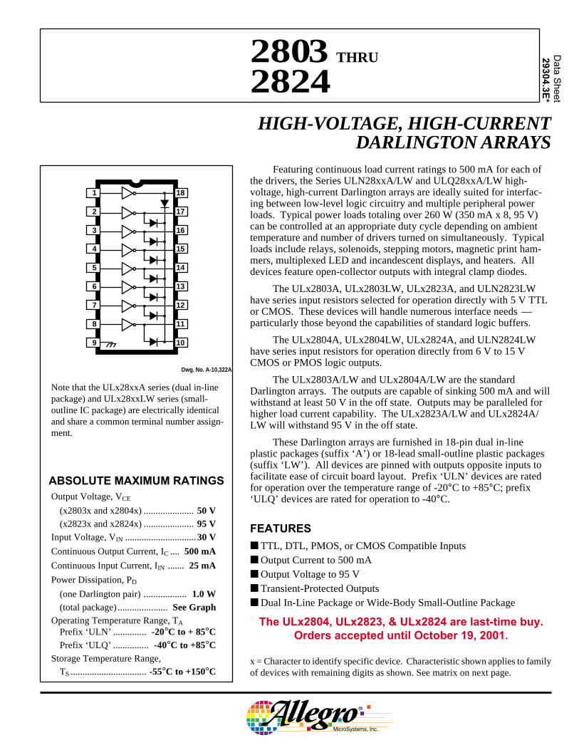
Featuring continuous load current ratings to 500 mA for each ofthe drivers, the Series ULN28xxA/LW and ULQ28xxA/LW high-voltage, high-current Darlington arrays are ideally suited for interfac-ing between low-level logic circuitry and multiple peripheral powerloads. Typical power loads totaling over 260 W (350 mA x 8, 95 V)can be controlled at an appropriate duty cycle depending on ambienttemperature and number of drivers turned on simultaneously. Typicalloads include relays, solenoids, stepping motors, magnetic print ham-mers, multiplexed LED and incandescent displays, and heaters. Alldevices feature open-collector outputs with integral clamp diodes.
The ULx2803A, ULx2803LW, ULx2823A, and ULN2823LWhave series input resistors selected for operation directly with 5 V TTLor CMOS. These devices will handle numerous interface needs —particularly those beyond the capabilities of standard logic buffers.
The ULx2804A, ULx2804LW, ULx2824A, and ULN2824LWhave series input resistors for operation directly from 6 V to 15 VCMOS or PMOS logic outputs.
The ULx2803A/LW and ULx2804A/LW are the standardDarlington arrays. The outputs are capable of sinking 500 mA and willwithstand at least 50 V in the off state. Outputs may be paralleled forhigher load current capability. The ULx2823A/LW and ULx2824A/LW will withstand 95 V in the off state.
These Darlington arrays are furnished in 18-pin dual in-lineplastic packages (suffix ‘A’) or 18-lead small-outline plastic packages(suffix ‘LW’). All devices are pinned with outputs opposite inputs tofacilitate ease of circuit board layout. Prefix ‘ULN’ devices are ratedfor operation over the temperature range of -20°C to +85°C; prefix‘ULQ’ devices are rated for operation to -40°C.
x = Character to identify specific device. Characteristic shown applies to familyof devices with remaining digits as shown. See matrix on next page.
2803 THRU
2824
18
17
15
14
13
7 12
8 11
9 10
1
2
4
5
6
Dwg. No. A-10,322A
163
ABSOLUTE MAXIMUM RATINGSOutput Voltage, VCE
(x2803x and x2804x) ..................... 50 V(x2823x and x2824x) ..................... 95 V
Input Voltage, VIN ..............................30 V
Continuous Output Current, IC .... 500 mA
Continuous Input Current, IIN ....... 25 mA
Power Dissipation, PD
(one Darlington pair) .................. 1.0 W(total package) ..................... See Graph
Operating Temperature Range, TA
Prefix ‘ULN’ .............. -20°C to + 85°CPrefix ‘ULQ’ ............... -40°C to +85°C
Storage Temperature Range,TS ................................ -55°C to +150°C
Note that the ULx28xxA series (dual in-linepackage) and ULx28xxLW series (small-outline IC package) are electrically identicaland share a common terminal number assign-ment.
The ULx2804, ULx2823, & ULx2824 are last-time buy.Orders accepted until October 19, 2001.

2803 THRU 2824HIGH-VOLTAGE,HIGH-CURRENTDARLINGTON ARRAYS
115 Northeast Cutoff, Box 15036Worcester, Massachusetts 01615-0036 (508) 853-50002
ULx28x4A/LW (Each Driver)
Copyright © 1977, 2001 Allegro MicroSystems, Inc.
VCE(MAX) 50 V 95 V
IC(MAX) 500 mA 500 mA
Logic Part Number
5V ULN2803A* ULN2823A*TTL, CMOS ULN2803LW* ULN2823LW
6-15 V ULN2804A* ULN2824A*CMOS, PMOS ULN2804LW* ULN2824LW
*Also available for operation between -40°C and +85°C. To order, changeprefix from ‘ULN’ to ‘ULQ’.
DEVICE PART NUMBER DESIGNATION
50 75 100 125 150
2.5
0.5
0
AMBIENT TEMPERATURE IN °C
2.0
1.5
1.0
25
Dwg. GP-018B
SUFFIX 'A', R = 60°C/WθJA
SUFFIX 'LW', R = 80°C/WθJA
AL
LO
WA
BL
E P
AC
KA
GE
PO
WE
R D
ISS
IPA
TIO
N IN
WA
TT
S
ULx28x3A/LW (Each Driver)
PARTIAL SCHEMATICS
x = Character to identify specific device. Specification shown applies tofamily of devices with remaining digits as shown. See matrix above.
The ULx2804, ULx2823, & ULx2824 are last-time buy.Orders accepted until October 19, 2001.
Dwg. FP-052-2
3 K
7.2 K
2.7 K
Dwg. FP-052-3
3 K
7.2 K
10.5 K

2803 THRU 2824HIGH-VOLTAGE,HIGH-CURRENT
DARLINGTON ARRAYS
www.allegromicro.com 3
Test Applicable Limits
Characteristic Symbol Fig. Devices Test Conditions Min. Typ. Max. Units
Output Leakage Current ICEX 1A All VCE = 50 V, TA = 25°C — < 1 50 µA
VCE = 50 V, TA = 70°C — < 1 100 µA
1B ULx2804x VCE = 50 V, TA = 70°C, VIN = 1.0 V — < 5 500 µA
Collector-Emitter VCE(SAT) 2 All IC = 100 mA, IB = 250 µA — 0.9 1.1 VSaturation Voltage lC = 200 mA, IB = 350 µA — 1.1 1.3 V
IC = 350 mA, IB = 500 µA — 1.3 1.6 V
Input Current IIN(ON) 3 ULx2803x VIN = 3.85 V — 0.93 1.35 mA
ULx2804x VIN = 5.0 V — 0.35 0.5 mA
VIN = 12 V — 1.0 1.45 mA
IIN(OFF) 4 All lC = 500 µA, TA = 70°C 50 65 — µA
Input Voltage VIN(ON) 5 ULx2803x VCE = 2.0 V, lC = 200 mA — — 2.4 V
VCE = 2.0 V, IC = 250 mA — — 2.7 V
VCE = 2.0 V, lC = 300 mA — — 3.0 V
ULx2804x VCE = 2.0 V, lC = 125 mA — — 5.0 V
VCE = 2.0 V, lC = 200 mA — — 6.0 V
VCE = 2.0 V, IC = 275 mA — — 7.0 V
VCE = 2.0 V, lC = 350 mA — — 8.0 V
Input Capacitance CIN — All — 15 25 pF
Turn-On Delay tPLH 8 All 0.5 EIN to 0.5 EOUT — 0.25 1.0 µs
Turn-Off Delay tPHL 8 All 0.5 EIN to 0.5 EOUT — 0.25 1.0 µs
Clamp Diode IR 6 All VR = 50 V, TA = 25°C — — 50 µALeakage Current VR = 50 V, TA = 70°C — — 100 µA
Clamp Diode VF 7 All IF = 350 mA — 1.7 2.0 VForward Voltage
Complete part number includes prefix to operating temperature range: ULN = -20°C to +85°C, ULQ = -40°C to +85°Cand a suffix to identify package style: A = DIP, LW = SOIC.
Types ULx2803A, ULx2803LW, ULx2804A, and ULx2804LWELECTRICAL CHARACTERISTICS at +25°C (unless otherwise noted).
The ULx2804 is last-time buy.Orders accepted until October 19, 2001.

2803 THRU 2824HIGH-VOLTAGE,HIGH-CURRENTDARLINGTON ARRAYS
115 Northeast Cutoff, Box 15036Worcester, Massachusetts 01615-0036 (508) 853-50004
Test Applicable Limits
Characteristic Symbol Fig. Devices Test Conditions Min. Typ. Max. Units
Output Leakage Current ICEX 1A All VCE = 95 V, TA = 25°C — < 1 50 µA
VCE = 95 V, TA = 70°C — < 1 100 µA
1B ULx2824x VCE = 95 V, TA = 70°C, VIN = 1.0 V — < 5 500 µA
Collector-Emitter VCE(SAT) 2 All IC = 100 mA, IB = 250 µA — 0.9 1.1 VSaturation Voltage lC = 200 mA, IB = 350 µA — 1.1 1.3 V
IC = 350 mA, IB = 500 µA — 1.3 1.6 V
Input Current IIN(ON) 3 ULx2823x VIN = 3.85 V — 0.93 1.35 mA
ULx2824x VIN = 5.0 V — 0.35 0.5 mA
VIN = 12 V — 1.0 1.45 mA
IIN(OFF) 4 All lC = 500 µA, TA = 70°C 50 65 — µA
Input Voltage VIN(ON) 5 ULx2823x VCE = 2.0 V, lC = 200 mA — — 2.4 V
VCE = 2.0 V, IC = 250 mA — — 2.7 V
VCE = 2.0 V, lC = 300 mA — — 3.0 V
ULx2824x VCE = 2.0 V, lC = 125 mA — — 5.0 V
VCE = 2.0 V, lC = 200 mA — — 6.0 V
VCE = 2.0 V, IC = 275 mA — — 7.0 V
VCE = 2.0 V, lC = 350 mA — — 8.0 V
Input Capacitance CIN — All — 15 25 pF
Turn-On Delay tPLH 8 All 0.5 EIN to 0.5 EOUT — 0.25 1.0 µs
Turn-Off Delay tPHL 8 All 0.5 EIN to 0.5 EOUT — 0.25 1.0 µs
Clamp Diode IR 6 All VR = 95 V, TA = 25°C — — 50 µALeakage Current VR = 95 V, TA = 70°C — — 100 µA
Clamp Diode VF 7 All IF = 350 mA — 1.7 2.0 VForward Voltage
Complete part number includes prefix to operating temperature range: ULN = -20°C to +85°C, ULQ = -40°C to +85°Cand a suffix to identify package style: A = DIP, LW = SOIC. Note that the ULQ2823LW and ULQ2824LW are not presentlyavailable.
Types ULx2823A, ULN2823LW, ULx2824A, and ULN2824LWELECTRICAL CHARACTERISTICS at +25°C (unless otherwise noted).
The ULx2823 & ULx2824 are last-time buy.Orders accepted until October 19, 2001.

2803 THRU 2824HIGH-VOLTAGE,HIGH-CURRENT
DARLINGTON ARRAYS
www.allegromicro.com 5
TEST FIGURES
Dwg. No. A-9732A Dwg. No. A-9733A Dwg. No. A-9734A
FIGURE 6 FIGURE 7 FIGURE 8
Dwg. No. A-9735A Dwg. No. A-9736A Vin
ULx28x3x 3.5 VULx28x4x 12 V
FIGURE 1A FIGURE 1B FIGURE 2
FIGURE 3 FIGURE 4 FIGURE 5
Dwg. No. A-9731ADwg. No. A-9730ADwg. No. A-9729A
OPEN
OPEN VCE
ICEX
µA
VIN
OPEN VCE
ICEX
µA
IB
OPEN
hFE =
VCE
V
ICIB
IC
VIN
OPEN
mA OPEN
IIN
OPEN VCE
IC
µA
IIN
µA
V
OPEN
VCE
VVIN
IC
OPEN
VR
IR
µAIF
OPENVF
V
PULSEGENERATORPRR = 10 kHz
DC = 50 %
INPUT93 Ω
100 Ω
50 pF30 Ω
OUT
+50 V
Dwg. EP-072

2803 THRU 2824HIGH-VOLTAGE,HIGH-CURRENTDARLINGTON ARRAYS
115 Northeast Cutoff, Box 15036Worcester, Massachusetts 01615-0036 (508) 853-50006
20
Dwg. GP-070-4
40 10080
DUTY CYCLE IN PER CENT
0
600
400
OU
TP
UT
CU
RR
EN
T IN
mA
/CH
AN
NE
L
200
060
NUMBER OF OUTPUTSCONDUCTING
SIMULTANEOUSLY TA = +50°CRθJA = 80°C/W
2
3
4
56
87
20
Dwg. GP-070-3
40 10080
DUTY CYCLE IN PER CENT
0
600
400
OU
TP
UT
CU
RR
EN
T IN
mA
/CH
AN
NE
L
200
060
NUMBER OF OUTPUTSCONDUCTING
SIMULTANEOUSLY
1
TA = +70°CRθJA = 80°C/W
8
3
4
67
5
2
ALLOWABLE COLLECTOR CURRENTAS A FUNCTION OF DUTY CYCLE
ULx28xxLW
20
Dwg. GP-070-2
40 10080
DUTY CYCLE IN PER CENT
0
600
400
OU
TP
UT
CU
RR
EN
T IN
mA
/CH
AN
NE
L
200
060
NUMBER OF OUTPUTSCONDUCTING
SIMULTANEOUSLY TA = +50°CRθJA = 60°C/W
2
3
4
56
87
20
Dwg. GP-070-1
40 10080
DUTY CYCLE IN PER CENT
0
600
400
OU
TP
UT
CU
RR
EN
T IN
mA
/CH
AN
NE
L
200
060
NUMBER OF OUTPUTSCONDUCTING
SIMULTANEOUSLY
1
TA = +70°CRθJA = 60°C/W
8
3
4
67
5
2
ALLOWABLE COLLECTOR CURRENTAS A FUNCTION OF DUTY CYCLE
ULx28xxA
x = Characters to identify specific device. Specification shown applies to family of devices with remaining digits as shown.

2803 THRU 2824HIGH-VOLTAGE,HIGH-CURRENT
DARLINGTON ARRAYS
www.allegromicro.com 7
INPUT CURRENT AS AFUNCTION OF INPUT VOLTAGE
ULx28x3x
3.0
Dwg. GP-069
5.0 6.0
INPUT VOLTAGE
2.0
2.5
2.0
INP
UT
CU
RR
EN
T IN
mA
— I
IN
1.0
0
MAXIMUM
0.5
1.5
4.0
AREA OF NORMAL OPERATIONWITH STANDARD OR SCHOTTKY TTL
TYPICAL
0.5
Dwg. GP-067
1.0 2.01.5
COLLECTOR-EMITTER SATURATION VOLTAGE
0
600
400
CO
LL
EC
TO
R C
UR
RE
NT
IN m
A
200
0
TYPI
CALM
AX. S
ATURAT
ION V
OLT
AGE
COLLECTOR CURRENT AS AFUNCTION OF INPUT CURRENT
200
Dwg. GP-068
400 600
INPUT CURRENT IN µA
0
600
400
CO
LL
EC
TO
R C
UR
RE
NT
IN m
A
200
0
MAX. REQ'D IN
PUT CURRENT
TYPIC
AL
ULx28x4x
6
Dwg. GP-069-1
10 12
INPUT VOLTAGE
5
2.0
INP
UT
CU
RR
EN
T IN
mA
— II
N
1.0
0
MAXIMUM
0.5
1.5
8
TYPICAL
7 9 11
SATURATION VOLTAGE AS A FUNCTION OFCOLLECTOR CURRENT
x = Characters to identify specific device. Characteristic shown applies to family of devices with remaining digits as shown.

2803 THRU 2824HIGH-VOLTAGE,HIGH-CURRENTDARLINGTON ARRAYS
115 Northeast Cutoff, Box 15036Worcester, Massachusetts 01615-0036 (508) 853-50008
PACKAGE DESIGNATOR “A” DIMENSIONSDimensions in Inches
(controlling dimensions)
Dimensions in Millimeters(for reference only)
NOTES:1. Exact body and lead configuration at vendor’s option within limits shown.2. Lead spacing tolerance is non-cumulative.3. Lead thickness is measured at seating plane or below.
0.0140.008
0.300BSC
Dwg. MA-001-18A in
0.430MAX
18
1 9
0.2800.240
0.210MAX
0.0700.045
0.015MIN
0.0220.014
0.100BSC
0.005MIN
0.1500.115
10
0.9200.880
0.3550.204
7.62BSC
Dwg. MA-001-18A mm
10.92MAX
18
1 9
7.116.10
5.33MAX
1.771.15
0.39MIN
0.5580.356
2.54BSC
0.13MIN
3.812.93
10
23.3722.35
2803 THRU 2824HIGH-VOLTAGE,HIGH-CURRENT
DARLINGTON ARRAYS
www.allegromicro.com 9
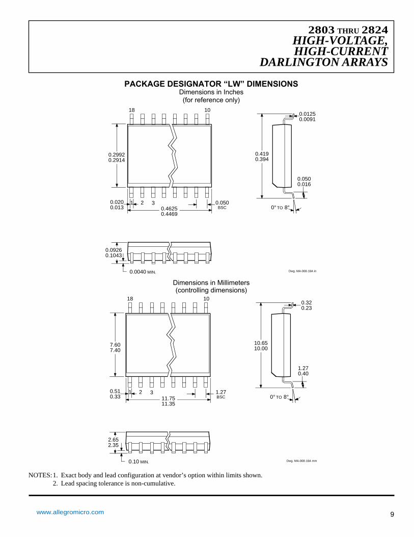
PACKAGE DESIGNATOR “LW” DIMENSIONSDimensions in Inches(for reference only)
Dimensions in Millimeters(controlling dimensions)
0° TO 8°1
18
2 30.510.33
0.10 MIN.
0.320.23
1.270.40
Dwg. MA-008-18A mm
1.27BSC
10
7.607.40
10.6510.00
11.7511.35
2.652.35
0° TO 8°1 2 30.020
0.013
0.0040 MIN.
0.01250.0091
0.0500.016
Dwg. MA-008-18A in
0.050BSC
18 10
0.4190.394
0.29920.2914
0.46250.4469
0.09260.1043
NOTES:1. Exact body and lead configuration at vendor’s option within limits shown.2. Lead spacing tolerance is non-cumulative.

2803 THRU 2824HIGH-VOLTAGE,HIGH-CURRENTDARLINGTON ARRAYS
115 Northeast Cutoff, Box 15036Worcester, Massachusetts 01615-0036 (508) 853-500010
The products described here are manufactured under one or moreU.S. patents or U.S. patents pending.
Allegro MicroSystems, Inc. reserves the right to make, from time totime, such departures from the detail specifications as may be requiredto permit improvements in the performance, reliability, ormanufacturability of its products. Before placing an order, the user iscautioned to verify that the information being relied upon is current.
Allegro products are not authorized for use as critical componentsin life-support devices or systems without express written approval.
The information included herein is believed to be accurate andreliable. However, Allegro MicroSystems, Inc. assumes no responsi-bility for its use; nor for any infringement of patents or other rights ofthird parties which may result from its use.
Top Related